Privacy statement: Your privacy is very important to Us. Our company promises not to disclose your personal information to any external company with out your explicit permission.
+86-0510-86199063
Multi-band CDMA and WCDMA mobile phones require greater RF design work to provide sufficient output power and ensure the normal operation of linearity and efficiency in each frequency band. The design usually includes a power amplifier and duplex for each frequency band, RF filters and switches to match multiple RF inputs to a single antenna. In order to reduce the complexity of multi-band mobile phone design, ANADIGICS has developed dual-band CDMA and WCDMA power amplifier modules. By integrating two power amplifier modules in a single package, compared with the previous DC and RF signal line design using two separate power amplifiers, the board area can be effectively reduced. This article will describe the typical application of dual-frequency power amplifier module in CDMA / EVDO and WCDMA / HSPA mobile phone design.
This article will focus on the design and application of ANADIGICS AWT6221 in the 2nd and 5th frequency bands of UMTS, dual-band WCDMA / HSPA. AWT6221 (see Figure 1) of ANANDIGICS has won the Outstanding Achievement Award for Information Technology Application and Communication Technology Innovation issued by the Ministry of Industry and Information Technology of China.

Figure 1. AWT6221
Compared with the general standard power amplifier, AWT6221 dual-frequency power amplifier greatly reduces the average current power consumption by up to 75%, and increases the talk time by up to 25%.
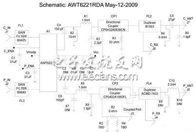
ANADIGICS 'HELP3 power amplifier, such as the AWT6221 power amplifier, uses the company's unique InGaP-Plus technology, and integrates HBT and pHEMT devices in the same BiFET wafer. With the optional bias mode, the HELP3 power amplifier exhibits the best efficiency in the low range and mid-range output power level. The AWT6221 smart bias circuit reduces current consumption to 8mA at low power levels. By integrating two independent power amplifier chains, the ultra-mini AWT6221 provides excellent performance in these two frequency bands and saves printed circuit board area, as shown in Figure 2.

Figure 2. AWT6221 reference design
AWT6221 is developed for dual band WCDMA / HSPA mobile phone UMTS Band 2 (824-849MH) and Band 5 (1850-1910MHz). 3GPP technology regulates the level 3 power of user equipment and must meet or exceed these minimum performance levels.
• Maximum output power: + 24dBm + 1 / -3 dBm
• Adjacent channel leakage power ratio (ACLR) +/- 5MHz: -33dBm
• Adjacent channel leakage power ratio (ACLR) +/- 10MHz: -43dBm
• Maximum harmonic emission specified frequency: 30 – 1000MHz: -36dBm / 100kHz
ο Between 1 -12.75GHz: -30dBm / 1MHz ο Between 869 – 894MHz: -60dBm / 3.84MHz ο Between 1930-1990MHz: -60dBm / 3.84MHz ο Between 2100-2170MHz: -60dBm / 3.84MHz between
The frequency division duplex system of most CDMA and WCDMA networks allows different radio frequency bands to be allocated to uplink (from mobile to base station) and downlink (from base station to mobile) at the same time. Duplexers are used in mobile devices to allow UL and DL to utilize a single antenna. In UMTS band 2, we chose Avago Technology's micro-FBAR duplex high-Q response ACMD-7403. For Band 5, we chose the Epcos low loss SAW duplex B-7663. The reference design also includes the coupled AVX of the CP402A thin film power directional coupler, which provides the required RF power for many top 3G chipsets.
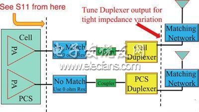
The development of the AWT6221 reference design started with the further coupling of the power amplifier and the measurement of duplex S-parameters. In this measurement, zero ohm resistance is used to shorten the matching components on the circuit board, see Figure 3.
The S parameter describes the voltage signal reflected by each port network of the N port. The subscript of the first number refers to the response port, while the second number refers to the event port. Therefore S21 refers to the reaction caused by the signal terminal 1 at port 2. The S parameter comes from a matrix port with equal number of rows and columns. The parameters along the diagonal of the S matrix are called reflection coefficients, and the diagonal S parameters are called transmission coefficients because they only occur at a single port. The two-port network of the S matrix is shown in the table below:

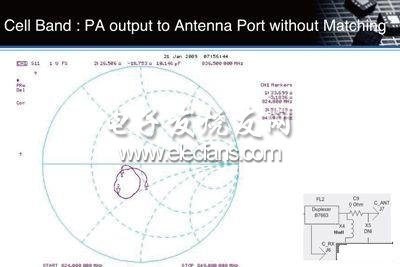
The reflection coefficient (S11) is tested against the frequency range of the RF path of Band 2 and Band 5. The power amplifier forms a series of impedance changes when it does not conform to the output of the circuit. The results are shown in the Smith table shown in Figure 4 and Figure 5.

Figure 4. Cell Band: PA output to Antenna Port without Matching
October 23, 2023
August 16, 2023
January 16, 2024
Email ke pemasok ini
October 23, 2023
August 16, 2023
January 16, 2024

Privacy statement: Your privacy is very important to Us. Our company promises not to disclose your personal information to any external company with out your explicit permission.

Fill in more information so that we can get in touch with you faster
Privacy statement: Your privacy is very important to Us. Our company promises not to disclose your personal information to any external company with out your explicit permission.